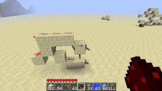
Video: Building a minecraft computer tutorial pt7: Readable/Writeable Memory with D flip-flops by bennyscube
How to build it
- Build the 2-Wide Inverter Decoder
Start by placing solid blocks in a staggered, 2-wide zigzag pattern to hold your NOT gates (redstone torches). Place redstone torches and dust along this path so that an incoming data signal is inverted and routed toward the memory stage without spilling into adjacent lanes.
- Construct the Vertical RS NOR Latch
At the output of the inverter section, build a vertical RS NOR latch to keep the whole circuit within the 2-wide footprint. Offset the upper and lower feedback blocks slightly rather than stacking them directly on top of each other so both inputs from the decoder can reach the latch.
- Connect the Decoder to the Latch
Run redstone dust from the two outputs of your inverter decoder directly into the set and reset inputs of the vertical RS NOR latch. This allows a single data line to either set or reset the latch depending on whether the input is on or off.
- Add the Write-Enable Line
Notice that the circuit only holds its stored value while the control wire stays powered. Place a redstone repeater facing into the control line to keep it locked by default, and attach your Write-Enable input before it so you can unpower the lock whenever you want to write new data.
- Place the Stabilization Repeater
Bend the feedback loop over the top of the latch and insert an extra redstone repeater along the upper wire. As shown in the video, this repeater prevents a redstone update quirk that would otherwise cause the latch to lose its state.
- Attach the Read Multiplexer (MUX)
At the output end of the D flip-flop, add two consecutive NOT gates (blocks with redstone torches) to double-invert the stored signal. Run a separate Read-Enable line into the intermediate inverter block so the stored bit only passes through to the final output line when the read line is triggered.
- Test Read and Write Operations
Place levers on the Data input, Write-Enable input, and Read-Enable input. Toggle the data lever, pulse the write lever to lock the bit into memory, and then switch on the read lever to verify that your stored 1 or 0 appears at the output.
How it works
This readable and writable memory cell breaks down into four distinct logical stages working in series:
- Inverter Decoder (3 NOT Gates): An RS NOR latch requires two separate lines (Set and Reset), whereas a D flip-flop takes a single Data (
D) input. The front-end NOT gates split and invert the single data input into both its original value and its inverse. - Write Enable Control: The control line under and behind the decoder forces the decoder torches off while powered, locking the latch in its current state. When you toggle the Write command, the lock releases and allows the current Data bit (
1or0) to flow into the latch. - Vertical RS NOR Latch: Two cross-coupled redstone torches arranged vertically store the bit indefinitely. One torch being ON forces the other OFF until the decoder forces a state change.
- Read Multiplexer (MUX): To prevent all memory cells from dumping their data onto a shared computer bus at once, the output passes through a torch inverter controlled by a Read line. Only when the Read signal unlocks the final torch does the stored
1or0pass out of the cell.
Tips & variations
- 2-Wide Tileable Footprint: Because the inverter chain and the RS NOR latch are built vertically inside a 2-block-wide profile, you can stack multiple cells side-by-side (with a 1-block gap or alternating repeaters) to create an 8-bit or 16-bit register.
- Don't Skip the Extra Repeater: If your latch forgets its state right after you turn off the write signal, make sure you included the extra repeater on the bent upper wire—without it, redstone update order issues can cause the torch loop to fail.
- WorldEdit / Structure Blocks: When copying this design to build larger RAM banks, double-check that you include the lowest layer of blocks and dust underneath the write line, and leave the Read MUX separate if you plan to wire a shared bus later.